Showing posts with label Logic. Show all posts

Monday, January 28, 2013

Electronics lessons: More on Logic gates

So a few months ago, I took a look at making gates with transistors
http://ah-screwit.blogspot.com/2012/10/electronics-lessons-making-gates.html

This post was a bit simplistic, but the logic was easy to follow, the idea that a transistor would conduct when on. (effectively being able to sink current from the output connecting the input of whatever came next to ground.) -or the transistor could be off, meaning not conducting so the output was connected to Vcc and the output was high.

This was the basic block of all the gates saying that we could run transistors in series to make the NOT gate into a NAND gate, or provide two connections to the base to make a NOR gate.

The trouble is, whilst in theory this will work, in practice there is not enough voltage gain, and over a series of make stages the signal will become weak.
The long and the short of it is that these simple single transistor gates are not real gates at all.

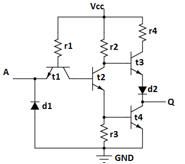
When I was talking about binary reduction and saving gates, you may think so what, I saved a NOT gate, that's only 1 transistor. but in reality. it's actually 4 transistors:

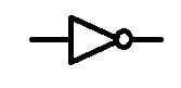
What you see here in a NOT gate.

It looks a little complicated and certainly the transistor T1 looks like it's connected the wrong way.

But it works a bit like this.
With a logic Low at the input.

T1 is clearly on, it's base is connected to Vcc,
Current flows from the base of T1 to the emitter, and flows to the logic low (ground).
the base of T2 is low, so T2 is off,
Since T2 is off we can see that the voltage at the emitter of T2 is low, so T4 is off, (output is not connected to ground through T4)
we can also see that since T2 is not conducting that the voltage at T2 collector is high, this is the base of T3, so T3 is on, conducting in the saturation region, and thus the output is high.

Logic low at input = Logic high at output.

Now consider what happens when the input is high.

T1 base is still connected to Vcc, so this transistor is still on and conducting, but this time rather than voltage flowing to ground at the input voltage must flow to ground through the base of T2, out the collector of T2, and to ground through R3.

so the Base of T2 is high, this turns T2 on.
this makes the T2 collector low and thus T3 it not on.
it makes the base of T4 high, so T4 is on. and connecting the output to ground.

logic high at input = logic low at output

So you see saving 80 not Gates doesn't save 80 transistors, it saves 320 transistors.

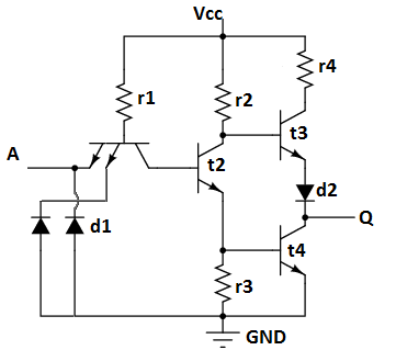
NAND
Funnily enough, with the basic transistor NAND gate we just stuck a transistor in series with the transistor making the NOT gate, now we put a second emitter in parallel with the first emitter.

We can't just put a transistor in series of parallel so we use a second emitter, (which is essentially just a second doped region on the silicon substrate.

This works exactly the same as the not gates, but instead of the base current for T2 being either grounded or supplied by THE (singular) input, it's not possible for it to be grounded by either input.

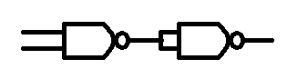
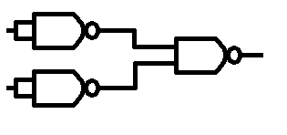
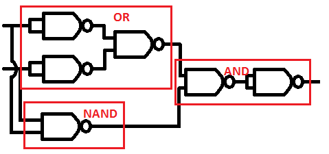
Again, an AND gate is made by connecting the output of a NAND gate to the input of a NOT gate.


Monday, October 29, 2012

Electronics lessons: Quine McCluskey

So I've looked at boolean algebra, and karnaugh maps.

What you may have realised is, first, binary systems become very big very fast.

But second, Boolean algebra, while useful has some pretty head churning limitations, feasibly there are no limitations, practically it's extraordinarily hard to be able to see what reductions may be created when dealing with more than three or four terms.

Karnaugh maps were a lot easier, yes they did require you to keep your wits about you whilst filling them in, the four by four map was filled logically as row 1 column1, row2 column1, row4 column 1, row 3 column 1. this carried on, but you filled column 1, then 2 then 4 then 3. so you sort of feel like you're jumping all over the place, and the logically last filled cell is at the middle of the table.

On top of that there is also the problem that karnaugh maps have a limitation on the amount of inputs that you can deal with practically, (it's difficult to use with a large number of inputs)

Now I'm going to briefly cover a algorithm called Quine McCluskey.

What makes this different is that it's expressed in a tabular formation. except rather than drawing boxes around the table we look for the number of ones in a given row where the output is true.

In order to demonstrate this I'm going to go back to the seven segment display. remember that first table that showed for each state 0 -15 what the 7 output segments on the 7 segment display needed to show;

0 = 0000 = 1 2 3    5 6 7
1 = 0001 =       3          7
2 = 0010 = 1    3 4 5 6
3 = 0011 = 1    3 4    6 7
4 = 0100 =    2 3 4       7
5 = 0101 = 1 2    4    6 7
6 = 0110 = 1 2    4 5 6 7
7 = 0111 = 1    3          7
8 = 1000 = 1 2 3 4 5 6 7
9 = 1001 = 1 2 3 4    6 7
a = 1010 = 1 2 3 4 5    7
b = 1011 = 1 2    4 5 6 7
c = 1100 = 1 2       5 6
d = 1101 =       3 4 5 6 7
e = 1110 = 1 2    4 5 6
f =  1111 = 1 2    4 5

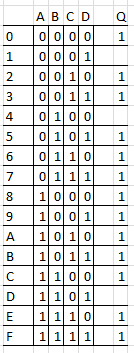
We'll start the demonstration of Quine McCluskey by looking at the table of outputs for segment 1 of the seven segment display.

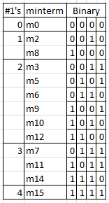
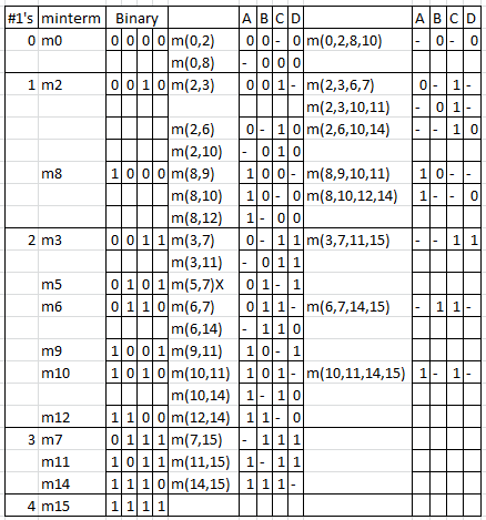
Then we draw a new table.
This table looks at the number of 1's in a state,
then the name of the state, (which is called a minterm)
and the binary representation of the state.

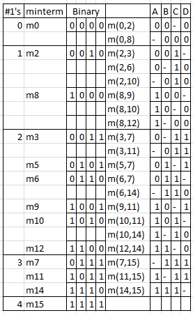
Now we look at the minterms and see which ones differ by only one bit.
Then we re-write these terms, using a dash to signify the bit that does not matter.

Look at minterms m14 (1110) and m15 (1111)
These are re-written as m(14 15) 111-

So you add these into that first table now, just a column along.
Mark any min term that cannot be combined, in this first case all minterms can be reduced.

OK, so now we have a table that has our first reduced minterms
It looks like we've got more work to do, yes it does look more complex than when we started, but honestly this is reducing the table!!

Now we need to combine our combined minterms.

To combine the minterms first we looked at where the states were just one bit out like m6[0110] and m14[1110]. became m(6, 14) [-110]
also m15[1111] and m7[0111] became m(7,15) [-111]

now we need to look at the conbined minterms where the dashes are in the same place and that only differ by one bit.

so:
m(6, 14) [-110]
m(7,15) [-111]

becomes
m(6, 7, 14, 15) [-11-]

We can conbine -010 and -110 or -011 or -000, as the dash is in the same place and they only differ by one bit
we can't combine -010 with -111 or -001 or -100 as there are two bits different, and we certainly can't combine -010 with -101 as that's three bit different.

We can't combine -010 with 001- as teh dash is in the wrong place for conbination

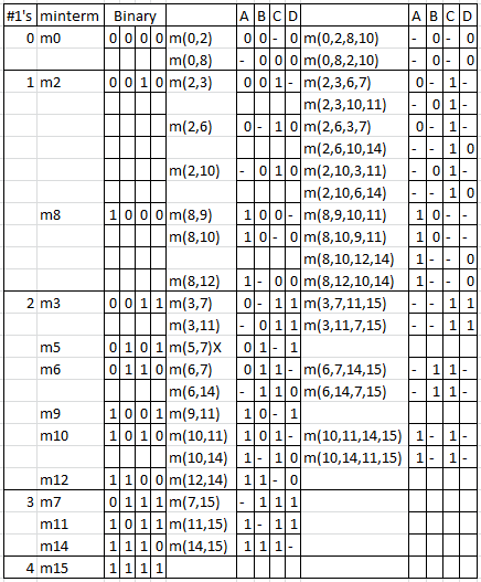
To start with just read down the chart and fill in ALL possibilities, we'll remove the repeated values later.

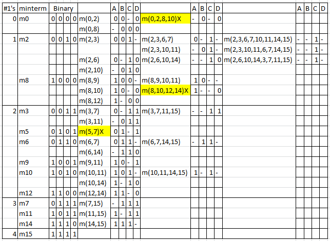
Now we can delete duplicates.

So the table has gotten a little smaller, and we can also see that m(5,7) is reduced as it's going to get. so we but an X next to this.

Now we start looking at the table to see where two dashes match but terms differ by only one value.

m(2,6,10,14) = [- - 1    0]
m(3,7,11,15) = [- - 1 1]

becomes m(2, 3, 6, 7, 10, 11, 14, 15) [ - - 1 - ]

In other words all of these terms can be reduced to the expression C

When you've finished matching the pairs your table should look like this:

now you can see that

m(2,3,6,7,10,11,14,15) - - 1 -
m(2,3,10,11,6,7,14,15) - - 1 - =>m(2,3,6,7,10,11,14,15) - - 1 -
m(2,6,10,14,3,7,11,15) - - 1 - =>m(2,3,6,7,10,11,14,15) - - 1 -

When we organise the minterms in numerical order

I highlighted the none combinable terms, and you can see that since we only have one term left there are no more combinations that can be made.

m(5,7)
m(8,10,12,14)
m(0,2,8,10)
m(2,3,6,7,10,11,14,15)

These minterms represent our prime implicants.
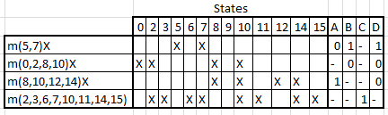
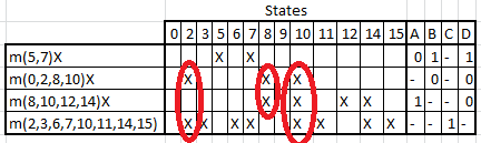
So now we draw a table listing the reduced/combined minterms from the table above.
The states, and their representations
This is called a prime implicant chart.

What this chart represents is the states that must be true.

This example doesn't lead well to what needs to happen next so for a moment pretend that the chart looks like this:

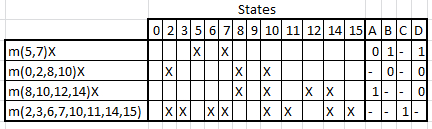
Now we can see that there is minterm2 that is common to two different outputs,
the 8 in the second statement can also be covered by one of the other statements, and the 10 can be covered too.

(so the statement relating to m(2,8,10) [-0-0]{/b./d} could be ignored as it would be covered in other statements.)

In this case where we have a statement that cannot be covered then it's an essential prime implicant, statements where the output states are covered by other statements are non-essential and can be left out.

Back in the real world we do have a minterm 0 on that second statement.

So it looks like they are ALL essential prime implicants.

so our output is m(5,7) OR m(0,2,8,10) OR m(8,10,12,14) + m(2,3,6,7,10,11,14,15)
looking at the values at the end this makes

m(5,7) = (/A . B .D) (the dash in C means C or NOT C, and as we know, A . B + A . /B = A

So we can write out the expression for the gates as:
Q1 = /A . B . D + /B . /D + A . /D + C

Monday, October 22, 2012

Electronics Lessons: Making Gates

So as promised in the last lessons I'm going to start to give a small idea of what these magical logic blocks are made up of. I'm going to draw out some very simplistic circuits that would work as basic logic gates using regular Bipolar Junction transistors.

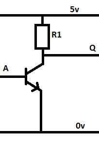
First we'll start with the NOT gate.

This circuit should look pretty familiar, because it's effectively the inverting amplifier that was made two years ago.

When the base of the transistor is bought high into the saturation region, the transistor conducts, and the collector is connected to ground.

When the base of the transistor is low, (in the cut-off region) the collector of the transistor is connected only to the Vcc voltage through the resistor, and thus the output of the circuit is high.


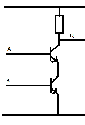
NAND
It might seem like it's going a little out of order to do the NAND gate next, but it's a very simple addittion to the NOT circuit.

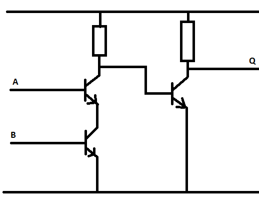
The NOT circuit pulls the output low by providing a path to ground when the transistor is on, the NAND gate works just like this, except there are two transistors that have to be on to provide that path to ground, and those transistors are in series.

(incidentally you could create an NOR gate by having the transistors in parallel)

AND
The output of the NAND gate is the inverse of the AND gate, and visa versa, to make an AND gate (when the output is high when both inputs are high) all we do it put a NOT gate following a NAND gate!

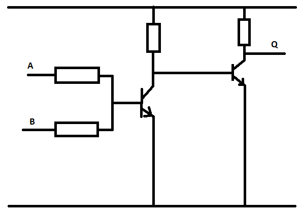
NOR
I said earlier that you could create a NOR gate just like a NAND gate, but instead of having the transistors in series have them in parallel.
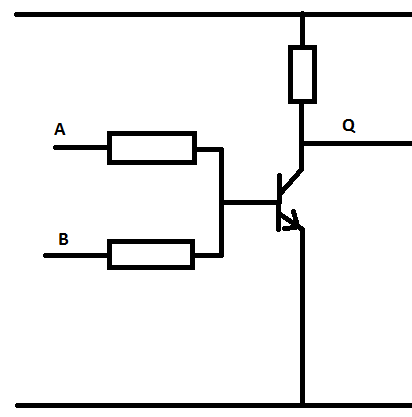
You can also just have the base of transistor 1 able to be brought high by either input.
in this scenario the inputs are isolated from each other with the use of resistors.

OR
Just as we turned a NAND gate into an AND gate with an inverter circuit (NOT gate) we do the same to turn the NOR gate into an OR gate.

With these basic gates it should be possible to make any logic circuit that you can imagine, (in fact this is possible with just the NAND gate as discussed in this blog post.
http://ah-screwit.blogspot.co.uk/2012/09/electronics-lessons-making-gates-from.html

Monday, October 15, 2012

Electronics lessons: Minimalism.

There is a saying that something is complete not when you've put everything that you can into it, but when you've taken everything that you can out of it.

In the last electronics lesson post I looked at creating a simple logic circuit for driving a seven segment display that would display the hex numerals 1 - F. the logic states were reduced using karnaugh maps to a minimalist form and the end circuit was a log circuit that would work very well as a binary - hex decoder.

However, the circuit drawn at the end was very inefficient, there were far more gates than were actually needed, when you consider that it costs time to make each gate, and materials, and die space, having a few extra hundred transistors on a piece of silicone might not sound like a lot, (perhaps it only costs  one tenth of one penny to make al lthe extra gates), but when you make millions of devices that soon adds up.

Imagine if the 555 timer had 50 odd extra transistors due to poor design that's a tenth of a penny, for a device that is sold in tens of millions per year, over nearly fifty years.

Sloppy design can cost a lot. if you were making the circuit not on silicone but out of discrete transistors, at a cost of £0.10 per transistor and extra 50 transistors makes your circuit £5 more expensive.


Minimising
So onto minimising the circuit that we made last time.

When we finished we were looking at:
Q1 = C + /D + (A. /B)
Q2 = (/C . /D) + (B . /D) + (A . C) + (A . /B) + (/A . B . /C)
Q3 = (/A . /B) + (/B . /C) + (/B . /D) + ( /A . /C . /D) + (/A . C . D) + (A . /C . D)
Q4 = (A . /B) + (C . /D) + (A . C) + (/B . C) + (/A . B . /C)
Q5 = (C . /D) + (/B . /D) + (A . B)
Q6 = (A . /C) + (/A . /B . /D) + (/B . C . D) + (B . /C . /D) + (B . C . /D)
Q7 = (A . /B) + (/A . B) + (B . C) + (/B . /C) + (/B . D)

as our logic circuit.

Now We can just build these logic circuits one on top of the other, 7 individual circuits, but we can see that some of the elements are the same across each statement for the output.

for example Q1 and Q2 both contain A . /B.
why build them as separate pods, why not build that block once and have it fed to the OR gate that will inevitably be at the output of both the Q1 and Q2 outputs?

So now we need to take our truth statements and look for common elements.
Working through that list also looking for common elements we find:

C = Q1***
/D = Q1***
(A. /B) = Q1, Q2, Q4 Q7
(/C . /D) = Q2, ***
(B . /D) = Q2, ***
(A . C) = Q2, Q4,
(/A . /B) = Q3***
(/B . /C) = Q3, Q7
(/B . /D) = Q3, Q5 ***
(C . /D) = Q4, Q5 ***
(/B . C) = Q4 ***
(A . B) = Q5
(A . /C) - Q6 ***
(/A . B) = Q7 ***
(B . C) = Q7 ***
(/B . D) = Q7 ***


Q2 >  (/A . B . /C)
Q3 >  ( /A . /C . /D) + (/A . C . D) + (A . /C . D)
Q4 >  (/A . B . /C)
Q6 > (/A . /B . /D) + (/B . C . D) + (B . /C . /D) + (B . C . /D)


You'll see that I've written out logical blocks A . /B is by far the most used block in this system, it's used by four different outputs, so instead of repeating this block four times I'll have this as a single block that gets connected to four different outputs.

in fact all the blocks marked with stars are used in some way in the remaining more complex gate arrangements of Q2, Q3, Q4 and Q6 that require 3 inputs)

Some of the blocks only appear to be used once, for example /C . /D only appears in Q2, but /A . /C . /D

you see that if I create a block for /c . /d and just use that in the gate arrangement for Q2 it's a waste, I have to create another block with /c and /d in it and feed these into an AND gate with /A.

So again, why not just re-use the block.

All inputs with stars have got elements that can be used in other gate arrangements.

So Lets divide our circuit into blocks, we can then interconnect the blocks to produce the minimum amount of gates required to build the system. Each building block will be an element that represents a state.

so A = 1 is a state,
B = 1 is a state
A . B is a state that is made up of the two states above.

The idea here is that we only create each state once. creating a state twice is a was of die space/transistors.


To start with we'll define blocks 1 - 4 as A, B, C and D

X1 = A
X2 = B
X3 = C
X4 = D

Then we find that we use /A /B /C and /D everywhere so we'll make use of these too.

X5 = /A
X6 = /B
X7 = /C
X8 = /D

Now we'll start looking at our common blocks.
A . /B seems to be our most common so we'll define this as building block 9

X9 = A . /B = X1 . X6

As we go, we'll remove the statement from the list of 7 output states needed, that way we can be sure that we do not needlessly remake any elements

Q1 =  
Q2 = (/C . /D) + (B . /D) + (A . C) +   + (/A . B . /C)
Q3 = (/A . /B) + (/B . /C) + (/B . /D) + ( /A . /C . /D) + (/A . C . D) + (A . /C . D)
Q4 =   + (C . /D) + (A . C) + (/B . C) + (/A . B . /C)
Q5 = (C . /D) + (/B . /D) + (A . B)
Q6 = (A . /C) + (/A . /B . /D) + (/B . C . D) + (B . /C . /D) + (B . C . /D)
Q7 =   + (/A . B) + (B . C) + (/B . /C) + (/B . D)

Next we'll take the output /C . /D and define this as X10
X10 = /C . /D = X7 . X8

this expression is also used in the output for Q3 (/A . /C . /D), and the output of Q6 (B . /C . /D)
so we'll define these as X11 and X12 respectively

X11 = (/A . /C . /D) = X5 . X10
X12 = (B . /C . /D) = X2 . X10

our X13 block will be B . /D this is used in Q2, and in Q6 (B . C . /D) which will be X14

X13 = B . /D = X2 . X8
X14 = (B . C . /D) = X13 . X3

Moving on we have A . C this is used in the output of Q2 and Q4 only (and is not re-used in the more complex gate arrangements)

X15 = A . C = X1 . X3

Moving further down the list we get to /A . /B this is used  in Q3 and in Q6 as a part of the condition /A . /B . /D
so...

X16 = /A . /B = X5 . X6
X17 = /A . /B . /DX16 . X8

The condition /B . /C is only used in Q3 and Q7 and forms block 18

X18 = /B . /C = X6 . X7

the next one on the list is interesting, /B . /D is starred, it was used in Q3 and Q5, and in one of the other more complex arrangements (Q6 /A . /B . /D) but we've already taken care of the more complex arrangement in Q6 with block X17, so we needn't worry about catering for this again. X19 therefore is only used for Q3 and Q5 outputs

X19 = /B . /D = X6 . X8

the next state is C . /D this is used in the output of Q4 and Q5, and used in the output of Q6 (when combined with another state). but we already have enough states made to cater for that complex arrangement (which is X14)

X20 = C . /D = X2 . X7

if you've been working through this on paper, removing terms from the original statements as the terms are devised into logic blocks you should now only have this written on your page:
Q1 =
Q2 = (/A . B . /C)
Q3 = (/A . C . D) + (A . /C . D)
Q4 = (/B . C) + (/A . B . /C)
Q5 = (A . B)
Q6 = (A . /C) + (/B . C . D)
Q7 = (/A . B) + (B . C) + (/B . D)

The next term that we're going assign a state value to, (to make it a building block) is /B . C this is used in the output of Q4, and in the  more complex statement in Q6 /B . C . D

X21 = /B . C = X6 . X3
X22 = /B . C . D = X21 . X4

Continuing down the list

X23 = A . B = X1 . X2

A . /C is used in output Q3 (with D) and in output Q6

X24 =  A . /C = X1 . X7
X25 = A . /C . D = X24 . X4

Then we have /A . B which is used in Q7 and the more complex statements in Q2 and Q4

X26 = /A . B = X5 . X2
X27 = /A . B . /C = X26 . X7

Then we have three non common terms remaining B . C, /B . D, /A . C . D

X28 = B . C = X2 . X3
X29 = /B . D = X6 . X4
X30 = /A . C . D = X5 . X3 . X4

Now we've defined terms as states, where some of the states are made up of other states.

You'll have noticed in the large rather large schematic there were 40 not gates, with this state based arrangements there will only be four as the outputs of states, X1, 2, 3, 4, 5, 6, 7,8 are common to other inputs they form a most basic building block which are used to build other blocks.
We've already at an instant reduced our gate count by 36 gates.

So let's have a look at how many transistors are being used now.


We take our logical statements are replace our logical expressions with our state expressions.
X1 = A
X2 = B
X3 = C
X4 = D
X5 = /A
X6 = /B
X7 = /C
X8 = /D
X9 = A . /B = X1 . X6
X10 = /C . /D = X7 . X8
X11 = (/A . /C . /D) = X5 . X10
X12 = (B . /C . /D) = X2 . X10
X13 = B . /D = X2 . X8
X14 = (B . C . /D) = X13 . X3
X15 = A . C = X1 . X3
X16 = /A . /B = X5 . X6
X17 = /A . /B . /D = X16 . X8
X18 = /B . /C = X6 . X7
X19 = /B . /D = X6 . X8
X20 = C . /D = X2 . X7
X21 = /B . C = X6 . X3
X22 = /B . C . D = X21 . X4
X23 = A . B = X1 . X2
X24 =  A . /C = X1 . X7
X25 = A . /C . D = X24 . X4
X26 = /A . B = X5 . X2
X27 = /A . B . /C = X26 . X7
X28 = B . C = X2 . X3
X29 = /B . D = X6 . X4
X30 = /A . C . D = X5 . X3 . X4

(after the first few transformations you have)

Q1 = X3 + X8 + X9
Q2 = (/C . /D) + (B . /D) + (A . C) + X9 + (/A . B . /C)
Q3 = (/A . /B) + (/B . /C) + (/B . /D) + ( /A . /C . /D) + (/A . C . D) + (A . /C . D)
Q4 = X9 + (C . /D) + (A . C) + (/B . C) + (/A . B . /C)
Q5 = (C . /D) + (/B . /D) + (A . B)
Q6 = (A . /C) + (/A . /B . /D) + (/B . C . D) + (B . /C . /D) + (B . C . /D)
Q7 = X9 + (/A . B) + (B . C) + (/B . /C) + (/B . D)

You can see the way that this pattern is forming, Q1 is just going to be three building blocks connected to an Or gate, the X9 building block is going to be used for three other statements, so as well as saving 40 NOT gates, we've saved another 3 AND gates and we've only applied this to three terms at present!

We end up with a list like this.
Q1 = X3 + X8 + X9
Q2 = X10 + X13 + X15 + X9 +X27
Q3 = X16 + X18 + X19 + X11 + X30 + X25
Q4 = X9 + X20 + X15 + X21 + X27
Q5 = X20 + X19 + X23
Q6 = X24 + X17 + X22 + X12 + X14
Q7 = X9 + X26 + X28 + X18 + X29

Now we can start drawing out our Schematic for our gate connections.

We start with A, B, C, D and we label these connections with the state that they are
X1, X2, X3, and X4.

We look at the expression for Q1
Q1 = X3 + X8 + X9

So immediately we can take the output X3 (c) and draw a long line over to where we'll put out final OR gate
Then we have X8, we look to our Key, X8 is /D, or /X4
so we take the output from X4, and feed this through a not gate, we label the new state after the not gate X8, and draw a long line over to where our OR gate will sit.
Finally we have X9.  X9 is defined as X1 . X6.
We have X1 already, so we just draw a line to where we're going to place out AND gate, then we look at how to make X6.
X6 is /X2 so we take our X2 output, add a NOT gate, (and label the output X6 ready for use later), then we take our state X6 and feed this into the same AND gate that we connected X1 to.

We label the output of that AND gate X9, and draw a line over to where we're placing our final OR gate.
We now have all three inputs for the OR gate required and so we can put the OR gate in place and label it's output Q1...

The continue for the other statements.
In the statement for Q2 remember when we get to the part that says X9, we already have X9, so rather than adding a new AND gate, we just add a wire, connectting the existing building block X9 to the final OR gate of Q2.
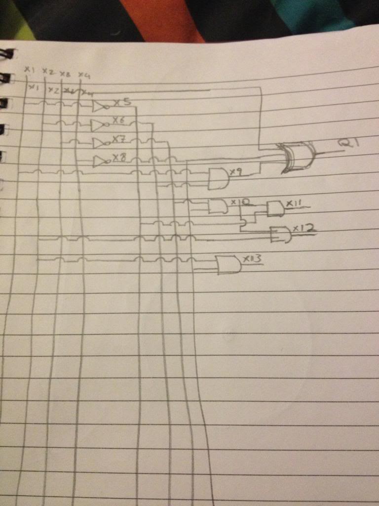
Drawing out the schematic can be an activity left to you.

There are 4 NOT Gates.
23 AND Gates 22 x 2 input gates plus 1 x 3 input AND gate.
and 7 OR gates of varying input size.

That's a reduction of 36 NOT gates, and 16 AND gates. (52 less gates).

Now that we've looked at taking really long and complicated statements such as:

Q1 = /a./b./c./d + /a./b.c./d + /a./b.c.d + /a.b/.c./d + /a.b.c./d + /a.b.c.d + a./b./c./d + a./b./c.d + a./b.c./d + a./b.c.d + a.b./c./d + a.b.c./d + a.b.c.d

and reducing them to:

Q1 = (A . /B) + C + /D

(If you blindly just drew gates for each expression on the first you'd use: 26 NOT gates, 39 (4 input) AND gates and a 12 input OR gates.)

The second statement uses 2 NOT gates, 1 AND gate and a 3 input OR gate.


The question is WHY that's important. you might be thinking I can afford to buy a chip, or a few extra chips with gates in them.
after all a chip with 4 x 2 input AND gates on it is only a few pence, you could even afford to use three of those gates to make your four input AND gate and just ignore the last gate.

But the point is that the expense adds up. for this single statement you can perform ALL the logic needed with just 3 devices, (an array of NOT gates, and array of AND gates, and an array of OR gates), also you'll have gates left over for use in the 7 other output states of the hex decoder.

A chip containing 6 NOT gates costs, £0.20 from Farnell. if you plan to use 25 not gates for this one statement then the costs is £1.20 as you need to buy 6 chips.

If you didn't reduce any of the statements you'd use loads more.

Earlier I looked at combining gate arrays to minimise the amount of gates required, and got the count down to just 4 NOT gates. -that's 1 chip.

So reduction saves £1 in this statement

when we look at the original statements in the making a hex counter the logic needed to drive a seven segment display was:

Q1 = /a./b./c./d + /a./b.c./d + /a./b.c.d + /a.b./c./d + /a.b.c./d + /a.b.c.d + a./b./c./d + a./b./c.d + a./b.c./d + a./b.c.d + a.b./c./d + a.b.c./d + a.b.c.d

Q2 = /a./b./c./d + /a.b./c./d + /a.b./c.d + /a.b.c./d + a./b./c./d + a./b./c.d + a./b.c./d + a./b.c.d + a.b./c./d + a.b.c./d + a.b.c.d

Q3 = /a./b./c./d + /a./b./c.d + /a./b.c./d + /a./b.c.d + /a.b./c./d + /a.b.c.d + a./b./c./d + a./b./c.d + a./b.c./d + a.b./c.d

Q4 = /a./b.c./d + /a./b.c.d + /a.b./c./d + /a.b./c.d + /a.b.c./d + a./b./c./d + a./b./c.d + a./b.c./d + a./b.c.d + a.b./c.d + a.b.c./d + a.b.c.d

Q5 = /a./b./c./d + /a./b.c./d + /a.b.c./d + a./b./c./d + a./b.c./d + a./b.c.d + a.b./c./d + a.b./c.d + a.b.c./d + a.b.c.d

Q6 = /a./b./c./d + /a./b.c./d + /a./b.c.d + /a.b./c.d + /a.b.c./d + a./b./c./d + a./b./c.d + a./b.c.d + a.b./c./d + a.b./c.d + a.b.c./d

Q7 = /a./b./c./d + /a./b./c.d + /a./b.c.d + /a.b./c./d + /a.b./c.d + /a.b.c./d + /a.b.c.d + a./b./c./d + a./b./c.d + a./b.c./d + a./b.c.d + a.b.c./d + a.b.c.d
there are 162 not gates used that's 27 chips £5.40 in chips.

this was reduced to 40 NOT gates (7 chips / £1.40 in chips)

by looking at a series of state machines as building blocks this was furter reduced to 4 NOT gates (£0.20)

Now consider that these surface mount chips containing the arrays of NOT gates are 6 x 9mm,
you'll need perhaps a border of 10mm around each chip to allow for the hundreds of traces that you're going to need to run inter connecting these gates and you end up at. 26 x 29mm

Now you have 27 of these.
That's roughly 150mm x 150mm of board estate needed just for NOT gates, (we still have AND, and OR gates to put into this!!) -well that's for 25 which is a nice 5x5 square...


But for the moment ignore the fact that you can buy chips as pre-made packages.

What if you were making this from Transistors, or what if you were the chip manufacturer making this binary - hex converter in a single package.

162 NOT gates,
240 AND gates,
7 multi input OR gates. (73 x 2 input or gates if you were building with chips)


In the next post I'm going to explain how to make gates from Transistors, this creates TTL (transistor - transistor logic) devices.

After this lesson is complete you'll appreciate why when using TTL it's important to be minimalist, and extra few hundred gates may mean hundreds and hundreds more transistors, and hundreds of extra resistors being fabricated too! this is the same as wasting circuit board space.
Just as it's expensive to make big circuit boards it's expensive to make big chips.
Monday, October 08, 2012

Electronics lessons: Displaying Hexadecimal values on a seven segment display.

All this logic stuff is getting a bit dry, sure, we're able to express systems as a function of inputs and outputs.
We can reduce using boolean algebra, we know how to use truth tables, Karnaugh maps turned out to be a great tool for quick reduction.

But so far we haven't actually designed a system at all...

In order to make the lesson a little more interesting I'm now going to design a logic array for taking a binary number, and displaying the output in hexadecimal.

To do this We're going to use a seven segment LED display.

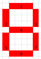
These displays are LED arrays arranged in a figure 8 shape, and can be used to express values by lighting LEDs.

We'll assign each bar of the display a value.

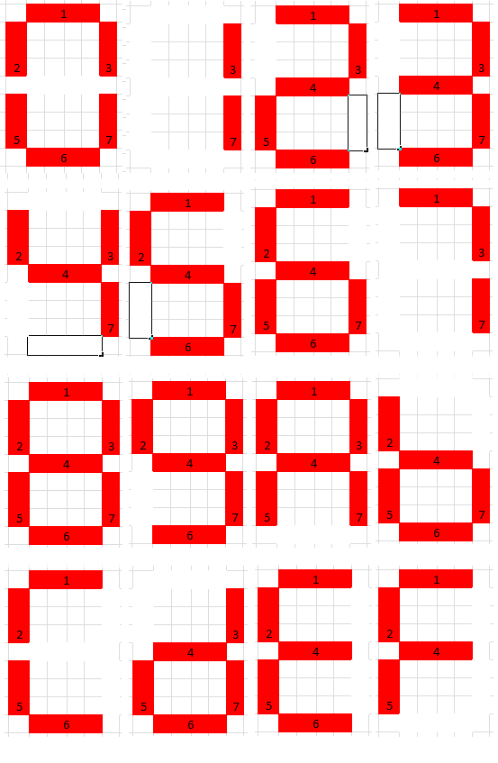
Then we can draw out what we want to display to show for each number.

We use this chart above to draw out a map of what we want our output states to be for any given input value.

To do this we draw a truth table, with input states, and our output states for the given input states.
From this truth table we can write out what logical expression we want each of our inputs to be on for.


0 = 0000 = 1 2 3    5 6 7
1 = 0001 =       3          7
2 = 0010 = 1    3 4 5 6
3 = 0011 = 1    3 4    6 7
4 = 0100 =    2 3 4       7
5 = 0101 = 1 2    4    6 7
6 = 0110 = 1 2    4 5 6 7
7 = 0111 = 1    3          7
8 = 1000 = 1 2 3 4 5 6 7
9 = 1001 = 1 2 3 4    6 7
a = 1010 = 1 2 3 4 5    7
b = 1011 = 1 2    4 5 6 7
c = 1100 = 1 2       5 6
d = 1101 =       3 4 5 6 7
e = 1110 = 1 2    4 5 6
f =  1111 = 1 2    4 5


so you can see that segment 1 of the display must be lit for states 0, 2, 3, 5, 6, 7, 8, 9, a, b, c, e and f

our inputs ABCD are listed for each state, so we write down the state of our inputs.

state 0 = /a . /b . /c . /d
state 2 = /a . /b . c . /d

So on and so fourth until we've got all 13 states.

then instead of saying Q1 = State0 OR state2...
we say:

Q1 = /a./b./c./d + /a./b.c./d + /a./b.c.d + /a.b/.c./d + /a.b.c./d + /a.b.c.d + a./b./c./d + a./b./c.d + a./b.c./d + a./b.c.d + a.b./c./d + a.b.c./d + a.b.c.d

We then continue this for the rest of the expected output states.
And reach the following statements:
Output        States
Q1 = 0 2 3 5 6 7 8 9 a b c e f
Q2 = 0 4 5 6 8 9 a b c e f
Q3 = 0 1 2 3 4 7 8 9 a d
Q4 = 2 3 4 5 6 8 9 a b d e f
Q5 = 0 2 6 8 a b c d e f
Q6 = 0 2 3 5 6 8 9 b c d e
Q7 = 0 1 3 4 5 6 7 8 9 a b e f


Q1 = /a./b./c./d + /a./b.c./d + /a./b.c.d + /a.b./c./d + /a.b.c./d + /a.b.c.d + a./b./c./d + a./b./c.d + a./b.c./d + a./b.c.d + a.b./c./d + a.b.c./d + a.b.c.d

Q2 = /a./b./c./d + /a.b./c./d + /a.b./c.d + /a.b.c./d + a./b./c./d + a./b./c.d + a./b.c./d + a./b.c.d + a.b./c./d + a.b.c./d + a.b.c.d

Q3 = /a./b./c./d + /a./b./c.d + /a./b.c./d + /a./b.c.d + /a.b./c./d + /a.b.c.d + a./b./c./d + a./b./c.d + a./b.c./d + a.b./c.d

Q4 = /a./b.c./d + /a./b.c.d + /a.b./c./d + /a.b./c.d + /a.b.c./d + a./b./c./d + a./b./c.d + a./b.c./d + a./b.c.d + a.b./c.d + a.b.c./d + a.b.c.d

Q5 = /a./b./c./d + /a./b.c./d + /a.b.c./d + a./b./c./d + a./b.c./d + a./b.c.d + a.b./c./d + a.b./c.d + a.b.c./d + a.b.c.d

Q6 = /a./b./c./d + /a./b.c./d + /a./b.c.d + /a.b./c.d + /a.b.c./d + a./b./c./d + a./b./c.d + a./b.c.d + a.b./c./d + a.b./c.d + a.b.c./d

Q7 = /a./b./c./d + /a./b./c.d + /a./b.c.d + /a.b./c./d + /a.b./c.d + /a.b.c./d + /a.b.c.d + a./b./c./d + a./b./c.d + a./b.c./d + a./b.c.d + a.b.c./d + a.b.c.d


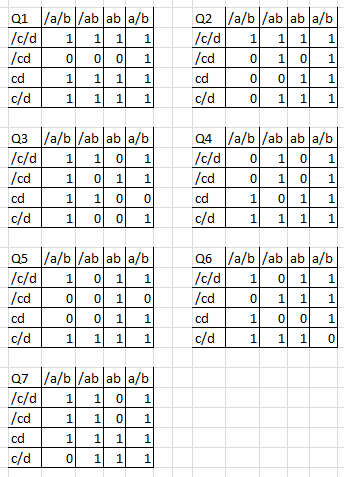
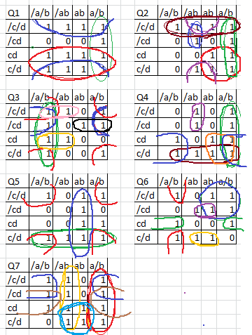
So now we can draw out the karnaugh maps for reducing these statements to their minimal form.

Then we start with looping groups of 1, 2, 4, 8 and 16.

Remembering that maps can loop around the top to the bottom, and that maps can loop left to right, and across the corners. (see Q3, Q5 and Q6 for an example of this):

Q1 = C + /D + (A. /B)
Q2 = (/C . /D) + (B . /D) + (A . C) + (A . /B) + (/A . B . /C)
Q3 = (/A . /B) + (/B . /C) + (/B . /D) + ( /A . /C . /D) + (/A . C . D) + (A . /C . D)
Q4 = (A . /B) + (C . /D) + (A . C) + (/B . C) + (/A . B . /C)
Q5 = (C . /D) + (/B . /D) + (A . B)
Q6 = (A . /C) + (/A . /B . /D) + (/B . C . D) + (B . /C . /D) + (B . C . /D)
Q7 = (A . /B) + (/A . B) + (B . C) + (/B . /C) + (/B . D)

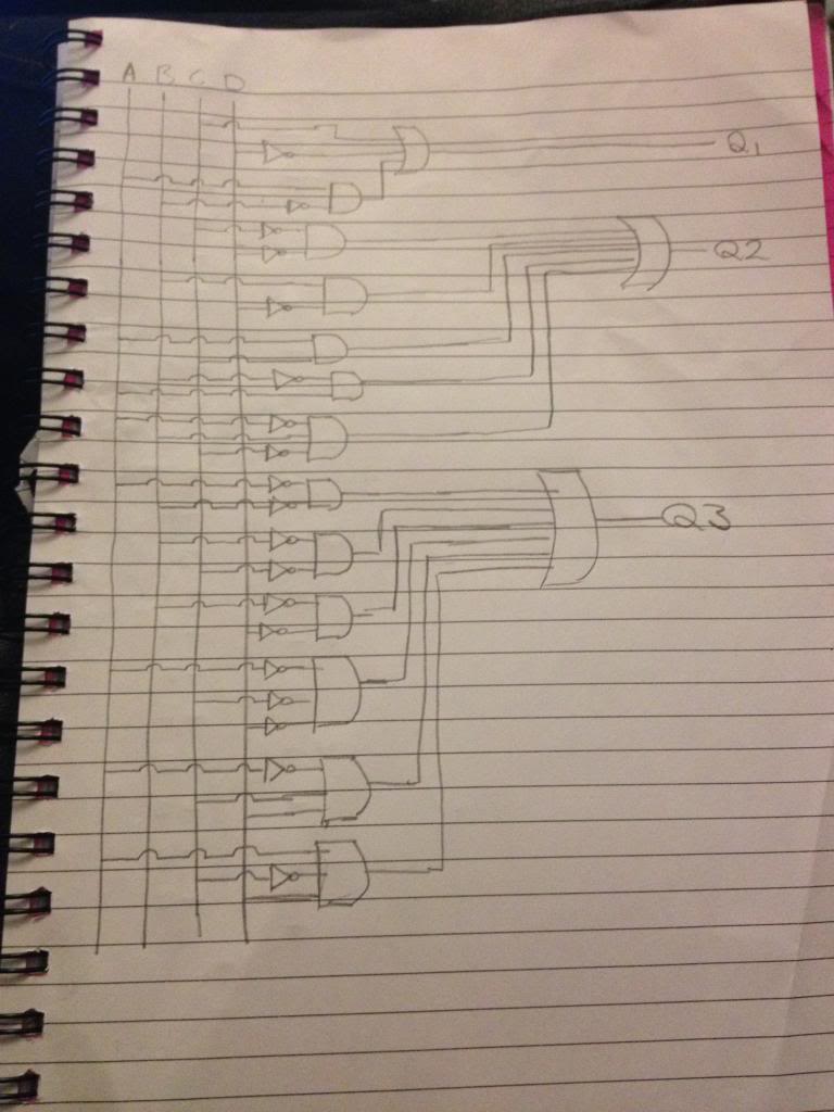
So now we'll build a schematic for this circuit.

There is a start for the first few outputs. feel free to finish it!

There are in total.
40 NOT gates
39 AND Gates, 31 x 2 input gates and 8 x 3 input gates
And of course 7 OR gates of varying input sizes

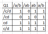
Note: After reviewing this I've noticed that there is a mistake for the output Q1.

This should have been minimised as so.


giving the final equation of Q1 = /A . B . D + /B . /D + A . /D + C

if you use the logic derrived in the first part of this post then you'll find that the output for Q1 on states 4 and 5 will be back to front.
e.g. the top bar will light for 4, making it look like a 9 without a tail.
the top bar will not light for 5 making it look like an upside down question mark
 

Monday, October 01, 2012

Electronics Lessons: Reducing logical expressions using Karnaguh maps.
Up to now I've talked about systems that have only a couple of inputs.
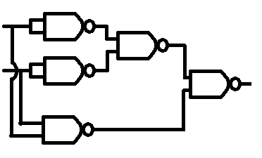
In this tutorial I'm going to look at designing a system that has two inputs, or three inputs, or four inputs.
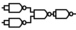
Karnaugh maps
Karnaugh maps are a design tool used for reducing binary expressions. the idea of a kanaugh maps is to look at the inputs to a system and the outputs of a system and write them down in such a way that they can be grouped together.

First we'll consider a very simple system.
We've got two inputs, (A and B)
We look at the system and we say.
when I apply logic 0 to input A, and logic 0 to input B the output Q is 0
when I apply logic 0 to input A, and logic 1 to input B the output Q is 0
when I apply logic 1 to input A, and logic 0 to input B the output Q is 0
when I apply logic 1 to input A, and logic 1 to input B the output Q is 1

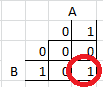
so we draw a table that is two columns wide, and 2 rows deep.
the columns are representing input A, whilst the rows represent input B.
in the table there are four spaces, these correspond to the output state.

We then Circle the input such that we group in blocks of 1, or 2 or 4 (in squares or rectangles.)

Here we've circles a block of 1.
This tells us the output is high for conditions of A . B, we've reduced the four statements into a single statement.


A different system may have the outputs
when I apply logic 0 to input A, and logic 0 to input B the output Q is 0
when I apply logic 0 to input A, and logic 1 to input B the output Q is 1
when I apply logic 1 to input A, and logic 0 to input B the output Q is 1
when I apply logic 1 to input A, and logic 1 to input B the output Q is 1

You see when we start making circles on the map this time there is two blocks of 2.

so our out put is high for conditions of A High, or conditions of B High.

We've reduced the map to A + B

2 input systems are a bit simple, and possibly faster to see worked out in your head faster than writing a map out.
however, as a system gets more complex adding more inputs they boolean algebra involved also gets more complex, and this is where karnaugh maps start to be really useful.

 Three Input Karnaugh Maps
Assume that we're dealing with a three input system where we have outputs for the following conditions.
(/a . /b . /c) + (/a . b . /c) + (/a . b . c) + (a . /b . c)
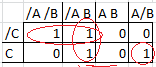
Now to draw this karnaugh map we use four columns along the top to show states of A nd B, with two rows to show what state C is.

But each column can only differ by one single value.
this means that you can change either input A OR in put A as you move across the columns, but not both at once.
so you can't go 00, 01 10, 11 the step from 01 to 10 changes A and B at the same time
so your column headers must go 00 01 11 10

You see in this Map there are two groups of two, and a single logic high on it's own.

This means that we can reduce the statement
(/a . /b . /c) + (/a . b . /c) + (/a . b . c) + (a . /b . c)
to
(/a . /c) + (/a . b) + (a . /b .c)


Four input Karnaugh maps
For a four input karnaugh map we must use inputs a, b, c and d this means we need four rows as well as four columns, though again each time the column must not differ by more than one value at a time.

In this example we'll use the logic statement.
Q1 = /a./b./c./d + /a./b.c./d + /a./b.c.d + /a.b./c./d + /a.b.c./d + /a.b.c.d + a./b./c./d + a./b./c.d + a./b.c./d + a./b.c.d + a.b./c./d + a.b.c./d + a.b.c.d

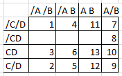
To fill in the karnaugh map we read through the statement filling in the corresponding box on the map where the statements match.

there are 13 parts of the statement;


1 /a./b./c./d +
2 /a./b.c./d +
3 /a./b.c.d +
4 /a.b./c./d +
5 /a.b.c./d +
6 /a.b.c.d +
7 a./b./c./d +
8 a./b./c.d
 9 a./b.c./d +
10 a./b.c.d +
11 a.b./c./d +
12 a.b.c./d +
13 a.b.c.d

so the map is filled in like so:

now we replace with ones and zeros...

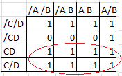
And we start grouping blocks of logic highs together. - grouping squares and rectangles of 1, 2, 4, 8, or 16 (obviously if we could group a block of 16 that's mean that the output was high no matter what.

We start by grouping the block of 8 at the bottom.

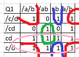
The common value here is C
we can see that when C is high the output of the system is high no matter what else happens in the system.

Now it looks like we have two groups of four left, (which would make the final statement, C . (/C . /D) + (A . /B)

But karnaugh maps can wrap around on themselves.
We make our loops to group logic highs where the inputs are only 1 value changed.
the first and fourth row only have 1 value changed (the value of C) so we create a loop that goes off the bottom of the table and comes back to the top.

So our logic statement is now C OR /D

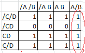
Now we look at the final block of grouped values, which is the column at the end.

The consistent values here are A . /B, C and D can be anything.

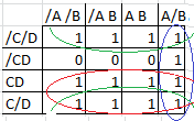
The complete map looks like this:

Leaving our complete logic statement as
Red loop conditions OR Green Loop conditions OR Blue loop conditions
C + /D + (A . /B)

Q1 = /a./b./c./d + /a./b.c./d + /a./b.c.d + /a.b./c./d + /a.b.c./d + /a.b.c.d + a./b./c./d + a./b./c.d + a./b.c./d + a./b.c.d + a.b./c./d + a.b.c./d + a.b.c.d
or Q1 = C + /D + (A . /B)

Which I'm sure you'll agree is a pretty fantastic reduction, from 13 conditions down to just 3.

Monday, September 17, 2012

Electronics Lessons: Making Gates from Gates

The most useful logic component that you'll ever find. -the NAND Gate.

So I've looked at logic gates and said that there are three Basic ones, AND, OR, NOT, that there is also an exclusive OR XOR, and that on top of that there is XNOR and NAND that can be made by adding a not gate to the end of the outputs.

We've had a peek at boolean algebra to show how things can be proven algebraically, and looked at truth tables to give a much more show and tell approach to showing binary states and logical outputs.

So now we'll look at how you can make any logic gate from a NAND gate.

We'll start by looking at the truth table for the NAND Gate

A B | Q
======
0 0 | 1
0 1 | 1
1 0 | 1
1 1 | 0

NOT
So lets start with the simplest functions.

Imagine that we connect both inputs together, so that inputs A and B are both the same,
now we're only concerned with states 0 and 3 on the truth table.

A B | Q
======
0 0 | 1
1 1 | 0

And it's only really a single input,

A | Q
====
0 | 1
1 | 0

Connecting both inputs of the NAND gate has made the NAND gate into a NOT gate.

AND
So how do we make a NAND gate an AND gate

A . B = //(A . B)
A . B = NOT NOT A AND B

yep, we just have the output of a two input NAND gate, connected to both inputs of a second two input NAND gate.

OR

Lets start with a truth table

A B | A + B | /A /B | /(/A . /B)
=======================
0 0 |    0    |  1  1  |    0
0 1 |    1    |  1  0  |    1
1 0 |    1    |  0  1  |    1
1 1 |    1    |  0  0  |    1

So first we make a couple of not gates, just like above, then we feed those to a NAND gate.

XOR
So we have our basic NOT, OR, AND gates all figured out, there is also the NAND gate already given (as that's out basic construction block)

Now we're going to look at XOR

To understand what XOR is I'll put the term into English.

XOR is, A or B, but not A and B

(A + B) . /(A . B)
Let's draw up the truth table for that one.


A B | XOR | OR | NAND | OR AND NAND
================================
0 0 |    0    |  0  |     1    |          0
0 1 |    1    |  1  |     1    |          1
1 0 |    1    |  1  |     1    |          1
1 1 |    0    |  1  |     0    |          0


XNOR

We can create an XNOR gate by adding a not gate to the end of our XOR gate, but Given that the last element is already a NOT gate, (NAND with conjoined inputs) rather than having two not gates back to back we can just remove the not gate already there.


NOR
And of course the NOR gate is just the OR gate with a NOT gate added to the end.


Monday, September 10, 2012

Electronics Lessons: Truth Tables

In the blog post that covered what logic functions there were I drew small tables that listed the input and showed what the output of a system would be.

In the Boolean algebra blog post I proved a weird looking rule with the using a couple of the little tables.

Those tables are called truth tables.

They depict what outputs occur as the conditions of an input.
You can use truth tables to prove logical statements.

Proving DeMorgan Theorem
As ever writing is nothing without context

So as an exercise in truth tables I'm going to look at the two rules of DeMorgan theorem.

These two rules are
/(A + B) = /A . /B
and
/(A. B) = /A + /B

This is easier to do on paper than it is on a computer screen writing in text, but here goes...

First we need to look at how many inputs we have,
We have A and B, so we need two columns.

Our first conditions are

NOT ( A OR B )

So to start with we'll draw the truth table for
A OR B

A B | Q1
=======
0 0 | 0
0 1 | 1
1 0 | 1
1 1 | 1

Then we need to apply the NOT operation to the output Q1
Q1 | /Q1
0 => 1
1 => 0
1 => 0
1 => 0

So we know that the output of the truth table for /(A+B) looks like 1, 0, 0, 0 (for states 0,1,2,3)

Now we'll investigate the truth table for /A . /B

Lets start with A AND B

A B | Q
======
0 0  | 0
0 1  | 0
1 0  | 0
1 0  | 1

But what about NOT A and NOT B

/A /B | Q
1    1  | 1
1    0  | 0
0    1  | 0
0    0  | 0

So we know that the output of the truth table for /A . /B looks like 1, 0, 0, 0 (for states 0,1,2,3)

It's the same.

For a more complex problem it might be better to draw everything out inside a single truth table:

We'll do this to prove Demorgans second rule:
/(A . B) = /A + /B


A B | /A /B | A . B | /(A.B) | /A + /B
===========================
0 0  |  1 1    |    0     |    1      |    1
0 1  |  1 0    |    0     |    1      |    1
1 0  |  0 1    |    0     |    1      |    1
1 1  |  0 0    |    1     |    0      |    0


You see that the last two columns are the the statements used in DeMorgan theorem, and they do indeed prove DeMorgan theorem is correct.


States.
One thing mentioned above was that the states of inputs could be assigned names.

Where you have defined input names that are ordered, A, B, C or In1, In2, In3 you can assign the different states values in accordance with the binary numbering system

A B C = State name
0 0 0 = 0
0 0 1 = 1
0 1 0 = 2
0 1 1 = 3
1 0 0 = 4
1 0 1 = 5
1 1 0 = 6
1 1 1 = 7

Monday, September 03, 2012

Electronics Lessons: Boolean Algebra

There is nothing that would turn a person off a subject more than the mention of algebra.

But, do bear with me.

As with ordinary algebra we'er using letter to represent something, but in this case we're using it to represent states on inputs compared to what ew want our output to be.

I introduced notation in the last post that describes how to write logical expressions.

So lets just straight in.

In real maths we know that 1 + 2 = 2 + 1, both are equal to three.
The same is true in boolean algebra,

1 + 0 = 0 + 1
1 . 0 = 0 . 1

Also it's pretty obvious that if I say A and A, that's just A, if I give you a choice A or A, that's not really a choice.

A . A = A
A + A = A

We can use brackets in boolean algebra just like we do in regular algebra.

That means that:
(A + B) + C = A + (B + C)
(A . B) . C = A . (B . C)

Brackets can be expanded out the same wat that they are in regular maths
So:
A . (B + C) = A . B + A . C
A + (B . C) = (A + B) . (A + C)


Then we have terms that just don't matter.
A + (A . B)
A or A and B.
well in either case for the given output A has to be high and the state of B does not matter.
so:
A + A . B = A
A . (A + B) = A

We use 0 to represent a logic low, and a to represent a logic 1.
0 + A = A
0 . A = 0

1 + A = 1
1 . A = A

/A + A = 1
/A . A = 0


Not only are terms that are the same redundant. (Like A or A)
But terms that have all the same terms, but include a NOT statement are also redundant.

A and B, OR A and NOT B.

A .B + A . /B = A
(A + B) . (A + /B) = A

(A + B) . (A + /B) => A . A + A . /B + A . B + B . /B
B . /B is equal to 0
A . A + A . /B + A . B + B . /B => A + A . /B + A . B + 0
And just as A + 0 = A the same is true of a complex expression.
A + A . /B + A . B + 0 => A + A . /B + A . B
As said earlier A and A or A and NOT B is just as good as saying A
A + A . /B + A . B => A + A => A


Some more rules are:
A + /A . B = A + B

To prove this let's look at a table showing the outputs.
first lets look at /A . B
A => /A B | Q
===========
0 => 1  0 | 0
0 => 1  1 | 1
1 => 0  0 | 0
1 => 0  1 | 0

Now we'll put that into a new table so that we can look at A + /A . B

A Q | Out
=======
0 0 | 0
0 1 | 1
1 0 | 1
1 0 | 1

and compare that to A OR B
A B | Q
======
0 0 | 0
0 1 | 1
1 0 | 1
1 1 | 1

it's the same (weird looking rule proven!)

we also have
A ( /A + B) = A . B

The last two rules are a special set called DeMorgans Theorem.

/(A + B) = /A . /B
and
/(A. B) = /A + /B


Monday, August 27, 2012

Electronics Lessons: Logic Notation

In the last post I looked at various gates.

Now we're going to look at the various notations that are used when writing out statements of what logic circuits do.

First, lets think about a binary circuit.

Basically we'll have at least one input, and at least one output.

We'll call our inputs a series of letters, starting with A, and out outputs will be assigned the letter Q, if there is more than one output we'll call it Q1 and Q2.

It's exactly the same notiation for all the logic operators if you call inputs In1, In2 and so on


So lets start with the four simple gates
NOT, AND, OR, XOR
/ . + ⊕

the NOT gate is a slash.

Q = /A
q = not A

Alternativly not can be represented by an apostraphy after the letter

Q = A'
1 = 0'
0 = 1'
1 = /0
0 = /1

The AND gate is represented by a dot.
Q = A.B

0 . 0 = 0
0 . 1 = 0
1 . 0 = 0
1 . 1 = 1

the OR gate is represented by a plus sign.

Q = A+B
0 + 0 = 0
0 + 1 = 1
1 + 0 = 1
1 + 1 = 1

and XOR is represented by a plus with a circle around it

Q = A⊕B
0 ⊕ 0 = 0
0 ⊕ 1 = 1
1 ⊕ 0 = 1
0 ⊕ 0 = 0

finally we make up logical expressions the same way as we made up the gates for more complicated gates.
a NAND gate was just an AND gate with a NOT gate following it.

Q' = A + B
/Q = A + B
Q = /(A + B)

NOR
Q' = A+B
/Q = A+B
Q = /(A+B)

XNOR
Q' = A⊕B
/Q = A⊕B
Q = /(A⊕B)

Monday, August 20, 2012

Electronics lessons: Logic gates

Logic gates are useful in digital electronics, in digital electronics there are generally no wave forms, there is two states, either logic high or logic low, on or off, 1 of 0.

when we work with binary data we have to have a way to deal with it.

that way of dealing with it is with the use of logic gates.

There are a few basic logic gates.

NOT, AND OR, and XOR.

First NOT
You have two basic states in binary, on or off, if it's not on, it's off, if it's not off, it's on.

the not gate works in the same way as that sentence,

if you put a 1 into a not gate, it's output is 0
if you put a 0 into a not gate, it's output is 1

A | Q
====
0 | 1
1 | 0


AND

The AND gate has two inputs and one output. for the output to be on, ALL inputs to the AND gate must be on, if either one of the inputs is low then the output will also be low.

Think of it like two switches in series, both switches must be on in order for it to work.

A B | Q
======
0 0 | 0
0 1 | 0
1 0 | 0
1 1 | 1

OR

Another basic logic gate is the OR gate. again this gate has two inputs, the out put will be on  if either input A OR input B is on.

A B | Q
======
0 0 | 0
0 1 | 1
1 0 | 1
1 1 | 1

XOR
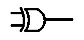
The last basic logic gate is the exclusive OR gate, XOR
With this gate the output will be on if In put A is high, OR if input B is on, but not if input A and input B is on. it must be exclusively A or B that is on, but definitely not A and B.

A B | Q
======
0 0 | 0
0 1 | 1
1 0 | 1
1 1 | 0


After this we start adding gates together to make more complicated logic gates.

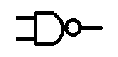
if we put a NOT gate after a AND gate we make a NAND gate we invert the input of a regular AND gate.

A B | Q
======
0 0 | 1
0 1 | 1
1 0 | 1
1 1 | 0

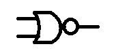
similarly we can make a NOR gate

A B | Q
======
0 0 | 1
0 1 | 0
1 0 | 0
1 1 | 0


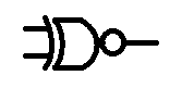
finally we have the Exclusive NOR gate XNOR

A B | Q
======
0 0 | 1
0 1 | 0
1 0 | 0
1 1 | 1