There is a saying that something is complete not when you've put everything that you can into it, but when you've taken everything that you can out of it.
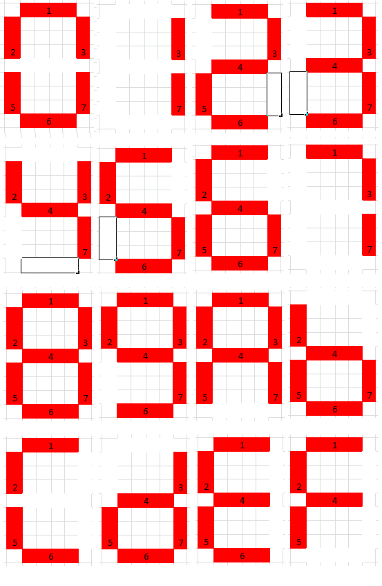
In the last electronics lesson post I looked at creating a simple logic circuit for driving a seven segment display that would display the hex numerals 1 - F. the logic states were reduced using karnaugh maps to a minimalist form and the end circuit was a log circuit that would work very well as a binary - hex decoder.
However, the circuit drawn at the end was very inefficient, there were far more gates than were actually needed, when you consider that it costs time to make each gate, and materials, and die space, having a few extra hundred transistors on a piece of silicone might not sound like a lot, (perhaps it only costs one tenth of one penny to make al lthe extra gates), but when you make millions of devices that soon adds up.
Imagine if the 555 timer had 50 odd extra transistors due to poor design that's a tenth of a penny, for a device that is sold in tens of millions per year, over nearly fifty years.
Sloppy design can cost a lot. if you were making the circuit not on silicone but out of discrete transistors, at a cost of £0.10 per transistor and extra 50 transistors makes your circuit £5 more expensive.
MinimisingSo onto minimising the circuit that we made last time.
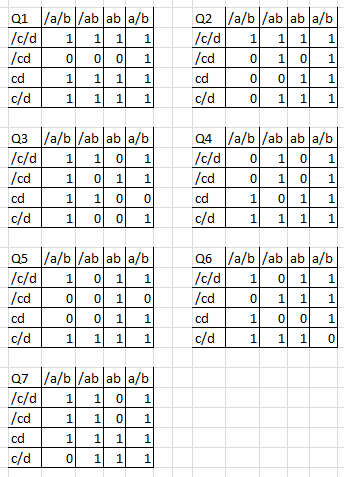
When we finished we were looking at:
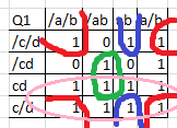
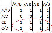
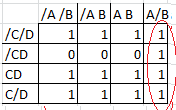
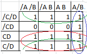
Q1 = C + /D + (A. /B)
Q2 = (/C . /D) + (B . /D) + (A . C) + (A . /B) + (/A . B . /C)
Q3 = (/A . /B) + (/B . /C) + (/B . /D) + ( /A . /C . /D) + (/A . C . D) + (A . /C . D)
Q4 = (A . /B) + (C . /D) + (A . C) + (/B . C) + (/A . B . /C)
Q5 = (C . /D) + (/B . /D) + (A . B)
Q6 = (A . /C) + (/A . /B . /D) + (/B . C . D) + (B . /C . /D) + (B . C . /D)
Q7 = (A . /B) + (/A . B) + (B . C) + (/B . /C) + (/B . D)
as our logic circuit.
Now We can just build these logic circuits one on top of the other, 7 individual circuits, but we can see that some of the elements are the same across each statement for the output.
for example Q1 and Q2 both contain A . /B.
why build them as separate pods, why not build that block once and have it fed to the OR gate that will inevitably be at the output of both the Q1 and Q2 outputs?
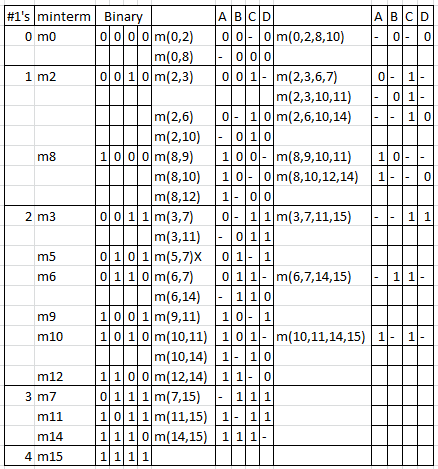
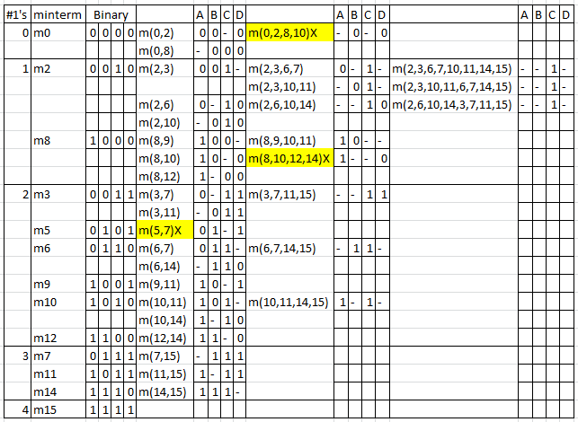
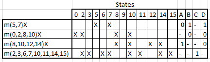
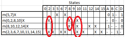
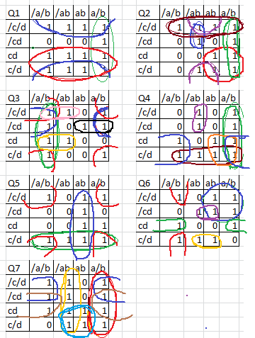
So now we need to take our truth statements and look for common elements.
Working through that list also looking for common elements we find:
C = Q1***
/D = Q1***
(A. /B) = Q1, Q2, Q4 Q7
(/C . /D) = Q2, ***
(B . /D) = Q2, ***
(A . C) = Q2, Q4,
(/A . /B) = Q3***
(/B . /C) = Q3, Q7
(/B . /D) = Q3, Q5 ***
(C . /D) = Q4, Q5 ***
(/B . C) = Q4 ***
(A . B) = Q5
(A . /C) - Q6 ***
(/A . B) = Q7 ***
(B . C) = Q7 ***
(/B . D) = Q7 ***
Q2 > (/A . B . /C)
Q3 > ( /A . /C . /D) + (/A . C . D) + (A . /C . D)
Q4 > (/A . B . /C)
Q6 > (/A . /B . /D) + (/B . C . D) + (B . /C . /D) + (B . C . /D)
You'll see that I've written out logical blocks A . /B is by far the most used block in this system, it's used by four different outputs, so instead of repeating this block four times I'll have this as a single block that gets connected to four different outputs.
in fact all the blocks marked with stars are used in some way in the remaining more complex gate arrangements of Q2, Q3, Q4 and Q6 that require 3 inputs)
Some of the blocks only appear to be used once, for example /C . /D only appears in Q2, but /A . /C . /D
you see that if I create a block for /c . /d and just use that in the gate arrangement for Q2 it's a waste, I have to create another block with /c and /d in it and feed these into an AND gate with /A.
So again, why not just re-use the block.
All inputs with stars have got elements that can be used in other gate arrangements.
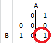
So Lets divide our circuit into blocks, we can then interconnect the blocks to produce the minimum amount of gates required to build the system. Each building block will be an element that represents a state.
so A = 1 is a state,
B = 1 is a state
A . B is a state that is made up of the two states above.
The idea here is that we only create each state once. creating a state twice is a was of die space/transistors.
To start with we'll define blocks 1 - 4 as A, B, C and D
X1 = A
X2 = B
X3 = C
X4 = D
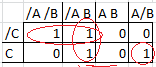
Then we find that we use /A /B /C and /D everywhere so we'll make use of these too.
X5 = /A
X6 = /B
X7 = /C
X8 = /D
Now we'll start looking at our common blocks.
A . /B seems to be our most common so we'll define this as building block 9
X9 = A . /B = X1 . X6
As we go, we'll remove the statement from the list of 7 output states needed, that way we can be sure that we do not needlessly remake any elements
Q1 =
Q2 = (/C . /D) + (B . /D) + (A . C) + + (/A . B . /C)
Q3 = (/A . /B) + (/B . /C) + (/B . /D) + ( /A . /C . /D) + (/A . C . D) + (A . /C . D)
Q4 = + (C . /D) + (A . C) + (/B . C) + (/A . B . /C)
Q5 = (C . /D) + (/B . /D) + (A . B)
Q6 = (A . /C) + (/A . /B . /D) + (/B . C . D) + (B . /C . /D) + (B . C . /D)
Q7 = + (/A . B) + (B . C) + (/B . /C) + (/B . D)
Next we'll take the output /C . /D and define this as X10
X10 = /C . /D = X7 . X8
this expression is also used in the output for Q3 (/A . /C . /D), and the output of Q6 (B . /C . /D)
so we'll define these as X11 and X12 respectively
X11 = (/A . /C . /D) = X5 . X10
X12 = (B . /C . /D) = X2 . X10
our X13 block will be B . /D this is used in Q2, and in Q6 (B . C . /D) which will be X14
X13 = B . /D = X2 . X8
X14 = (B . C . /D) = X13 . X3
Moving on we have A . C this is used in the output of Q2 and Q4 only (and is not re-used in the more complex gate arrangements)
X15 = A . C = X1 . X3
Moving further down the list we get to /A . /B this is used in Q3 and in Q6 as a part of the condition /A . /B . /D
so...
X16 = /A . /B = X5 . X6
X17 = /A . /B . /DX16 . X8
The condition /B . /C is only used in Q3 and Q7 and forms block 18
X18 = /B . /C = X6 . X7
the next one on the list is interesting, /B . /D is starred, it was used in Q3 and Q5, and in one of the other more complex arrangements (Q6 /A . /B . /D) but we've already taken care of the more complex arrangement in Q6 with block X17, so we needn't worry about catering for this again. X19 therefore is only used for Q3 and Q5 outputs
X19 = /B . /D = X6 . X8
the next state is C . /D this is used in the output of Q4 and Q5, and used in the output of Q6 (when combined with another state). but we already have enough states made to cater for that complex arrangement (which is X14)
X20 = C . /D = X2 . X7
if you've been working through this on paper, removing terms from the original statements as the terms are devised into logic blocks you should now only have this written on your page:
Q1 =
Q2 = (/A . B . /C)
Q3 = (/A . C . D) + (A . /C . D)
Q4 = (/B . C) + (/A . B . /C)
Q5 = (A . B)
Q6 = (A . /C) + (/B . C . D)
Q7 = (/A . B) + (B . C) + (/B . D)
The next term that we're going assign a state value to, (to make it a building block) is /B . C this is used in the output of Q4, and in the more complex statement in Q6 /B . C . D
X21 = /B . C = X6 . X3
X22 = /B . C . D = X21 . X4
Continuing down the list
X23 = A . B = X1 . X2
A . /C is used in output Q3 (with D) and in output Q6
X24 = A . /C = X1 . X7
X25 = A . /C . D = X24 . X4
Then we have /A . B which is used in Q7 and the more complex statements in Q2 and Q4
X26 = /A . B = X5 . X2
X27 = /A . B . /C = X26 . X7
Then we have three non common terms remaining B . C, /B . D, /A . C . D
X28 = B . C = X2 . X3
X29 = /B . D = X6 . X4
X30 = /A . C . D = X5 . X3 . X4
Now we've defined terms as states, where some of the states are made up of other states.
You'll have noticed in the large rather large schematic there were 40 not gates, with this state based arrangements there will only be four as the outputs of states, X1, 2, 3, 4, 5, 6, 7,8 are common to other inputs they form a most basic building block which are used to build other blocks.
We've already at an instant reduced our gate count by 36 gates.
So let's have a look at how many transistors are being used now.
We take our logical statements are replace our logical expressions with our state expressions.
X1 = A
X2 = B
X3 = C
X4 = D
X5 = /A
X6 = /B
X7 = /C
X8 = /D
X9 = A . /B = X1 . X6
X10 = /C . /D = X7 . X8
X11 = (/A . /C . /D) = X5 . X10
X12 = (B . /C . /D) = X2 . X10
X13 = B . /D = X2 . X8
X14 = (B . C . /D) = X13 . X3
X15 = A . C = X1 . X3
X16 = /A . /B = X5 . X6
X17 = /A . /B . /D = X16 . X8
X18 = /B . /C = X6 . X7
X19 = /B . /D = X6 . X8
X20 = C . /D = X2 . X7
X21 = /B . C = X6 . X3
X22 = /B . C . D = X21 . X4
X23 = A . B = X1 . X2
X24 = A . /C = X1 . X7
X25 = A . /C . D = X24 . X4
X26 = /A . B = X5 . X2
X27 = /A . B . /C = X26 . X7
X28 = B . C = X2 . X3
X29 = /B . D = X6 . X4
X30 = /A . C . D = X5 . X3 . X4
(after the first few transformations you have)
Q1 = X3 + X8 + X9
Q2 = (/C . /D) + (B . /D) + (A . C) + X9 + (/A . B . /C)
Q3 = (/A . /B) + (/B . /C) + (/B . /D) + ( /A . /C . /D) + (/A . C . D) + (A . /C . D)
Q4 = X9 + (C . /D) + (A . C) + (/B . C) + (/A . B . /C)
Q5 = (C . /D) + (/B . /D) + (A . B)
Q6 = (A . /C) + (/A . /B . /D) + (/B . C . D) + (B . /C . /D) + (B . C . /D)
Q7 = X9 + (/A . B) + (B . C) + (/B . /C) + (/B . D)
You can see the way that this pattern is forming, Q1 is just going to be three building blocks connected to an Or gate, the X9 building block is going to be used for three other statements, so as well as saving 40 NOT gates, we've saved another 3 AND gates and we've only applied this to three terms at present!
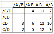
We end up with a list like this.
Q1 = X3 + X8 + X9
Q2 = X10 + X13 + X15 + X9 +X27
Q3 = X16 + X18 + X19 + X11 + X30 + X25
Q4 = X9 + X20 + X15 + X21 + X27
Q5 = X20 + X19 + X23
Q6 = X24 + X17 + X22 + X12 + X14
Q7 = X9 + X26 + X28 + X18 + X29
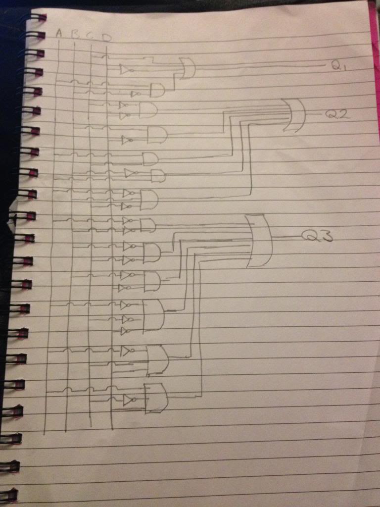
Now we can start drawing out our Schematic for our gate connections.
We start with A, B, C, D and we label these connections with the state that they are
X1, X2, X3, and X4.
We look at the expression for Q1
Q1 = X3 + X8 + X9
So immediately we can take the output X3 (c) and draw a long line over to where we'll put out final OR gate
Then we have X8, we look to our Key, X8 is /D, or /X4
so we take the output from X4, and feed this through a not gate, we label the new state after the not gate X8, and draw a long line over to where our OR gate will sit.
Finally we have X9. X9 is defined as X1 . X6.
We have X1 already, so we just draw a line to where we're going to place out AND gate, then we look at how to make X6.
X6 is /X2 so we take our X2 output, add a NOT gate, (and label the output X6 ready for use later), then we take our state X6 and feed this into the same AND gate that we connected X1 to.
We label the output of that AND gate X9, and draw a line over to where we're placing our final OR gate.
We now have all three inputs for the OR gate required and so we can put the OR gate in place and label it's output Q1...
The continue for the other statements.
In the statement for Q2 remember when we get to the part that says X9, we already have X9, so rather than adding a new AND gate, we just add a wire, connectting the existing building block X9 to the final OR gate of Q2.
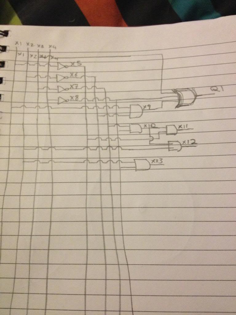
Drawing out the schematic can be an activity left to you.
There are 4 NOT Gates.
23 AND Gates 22 x 2 input gates plus 1 x 3 input AND gate.
and 7 OR gates of varying input size.
That's a reduction of 36 NOT gates, and 16 AND gates. (52 less gates).
Now that we've looked at taking really long and complicated statements such as:
Q1 = /a./b./c./d + /a./b.c./d + /a./b.c.d + /a.b/.c./d + /a.b.c./d + /a.b.c.d + a./b./c./d + a./b./c.d + a./b.c./d + a./b.c.d + a.b./c./d + a.b.c./d + a.b.c.d
and reducing them to:
Q1 = (A . /B) + C + /D
(If you blindly just drew gates for each expression on the first you'd use: 26 NOT gates, 39 (4 input) AND gates and a 12 input OR gates.)
The second statement uses 2 NOT gates, 1 AND gate and a 3 input OR gate.
The question is WHY that's important. you might be thinking I can afford to buy a chip, or a few extra chips with gates in them.
after all a chip with 4 x 2 input AND gates on it is only a few pence, you could even afford to use three of those gates to make your four input AND gate and just ignore the last gate.
But the point is that the expense adds up. for this single statement you can perform ALL the logic needed with just 3 devices, (an array of NOT gates, and array of AND gates, and an array of OR gates), also you'll have gates left over for use in the 7 other output states of the hex decoder.
A chip containing 6 NOT gates costs, £0.20 from Farnell. if you plan to use 25 not gates for this one statement then the costs is £1.20 as you need to buy 6 chips.
If you didn't reduce any of the statements you'd use loads more.
Earlier I looked at combining gate arrays to minimise the amount of gates required, and got the count down to just 4 NOT gates. -that's 1 chip.
So reduction saves £1 in this statement
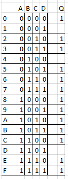
when we look at the original statements in the making a hex counter the logic needed to drive a seven segment display was:
Q1 = /a./b./c./d + /a./b.c./d + /a./b.c.d + /a.b./c./d + /a.b.c./d + /a.b.c.d + a./b./c./d + a./b./c.d + a./b.c./d + a./b.c.d + a.b./c./d + a.b.c./d + a.b.c.d
Q2 = /a./b./c./d + /a.b./c./d + /a.b./c.d + /a.b.c./d + a./b./c./d + a./b./c.d + a./b.c./d + a./b.c.d + a.b./c./d + a.b.c./d + a.b.c.d
Q3 = /a./b./c./d + /a./b./c.d + /a./b.c./d + /a./b.c.d + /a.b./c./d + /a.b.c.d + a./b./c./d + a./b./c.d + a./b.c./d + a.b./c.d
Q4 = /a./b.c./d + /a./b.c.d + /a.b./c./d + /a.b./c.d + /a.b.c./d + a./b./c./d + a./b./c.d + a./b.c./d + a./b.c.d + a.b./c.d + a.b.c./d + a.b.c.d
Q5 = /a./b./c./d + /a./b.c./d + /a.b.c./d + a./b./c./d + a./b.c./d + a./b.c.d + a.b./c./d + a.b./c.d + a.b.c./d + a.b.c.d
Q6 = /a./b./c./d + /a./b.c./d + /a./b.c.d + /a.b./c.d + /a.b.c./d + a./b./c./d + a./b./c.d + a./b.c.d + a.b./c./d + a.b./c.d + a.b.c./d
Q7 = /a./b./c./d + /a./b./c.d + /a./b.c.d + /a.b./c./d + /a.b./c.d + /a.b.c./d + /a.b.c.d + a./b./c./d + a./b./c.d + a./b.c./d + a./b.c.d + a.b.c./d + a.b.c.d
there are 162 not gates used that's 27 chips £5.40 in chips.
this was reduced to 40 NOT gates (7 chips / £1.40 in chips)
by looking at a series of state machines as building blocks this was furter reduced to 4 NOT gates (£0.20)
Now consider that these surface mount chips containing the arrays of NOT gates are 6 x 9mm,
you'll need perhaps a border of 10mm around each chip to allow for the hundreds of traces that you're going to need to run inter connecting these gates and you end up at. 26 x 29mm
Now you have 27 of these.
That's roughly 150mm x 150mm of board estate needed just for NOT gates, (we still have AND, and OR gates to put into this!!) -well that's for 25 which is a nice 5x5 square...
But for the moment ignore the fact that you can buy chips as pre-made packages.
What if you were making this from Transistors, or what if you were the chip manufacturer making this binary - hex converter in a single package.
162 NOT gates,
240 AND gates,
7 multi input OR gates. (73 x 2 input or gates if you were building with chips)
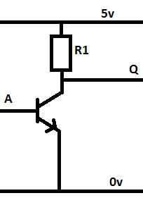
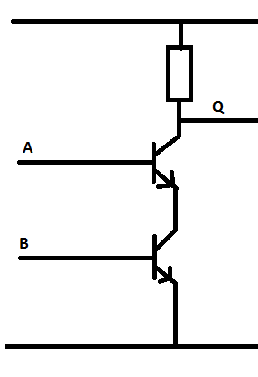
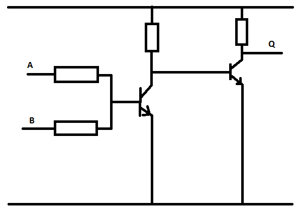
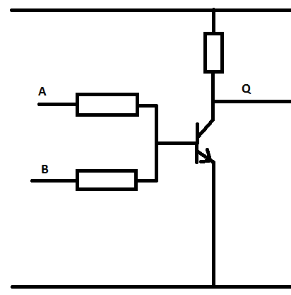
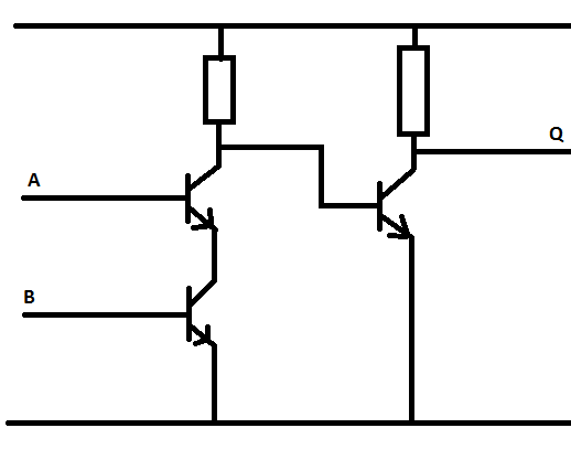
In the next post I'm going to explain how to make gates from Transistors, this creates TTL (transistor - transistor logic) devices.
After this lesson is complete you'll appreciate why when using TTL it's important to be minimalist, and extra few hundred gates may mean hundreds and hundreds more transistors, and hundreds of extra resistors being fabricated too! this is the same as wasting circuit board space.
Just as it's expensive to make big circuit boards it's expensive to make big chips.