This lesson deals exclusively with Bi-Polar Junction transistors (BJT)So I covered the diode, a couple of lessons ago.
I'm trying to make these lessons as simple as possible,
I'm trying to keep these beginner introductions to components as simple as possible, trying to keep them at a type GSCE level, so I'm not going to go into exactly how silicon is created and doped to P or N types, I'm not going to go through all the in depth technical stuff that a university course would cover.
These are beginner lessons, assuming that I do stick with this, those more in depth lessons should come a bit later.
The DiodeWhile I did just say that I wasn't going to go in depth as to how diodes are made it's important to understand a little bit about diodes.
Basically there are three types of silicon in this world.
There is silicon as you find it, that's pretty useless for electronics, then there is doped silicon, doping silicon enables to to be able to transport electrons and therefore allow electricity to flow.
There are two types of silicon, P type, (that contains what we call holes as the transport mechanism) and N type (that contains negative charge carriers [electrons]).
When you put these together you form a PN junction diode, which lets electricity flow one way.
The Transistor
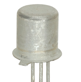
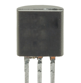
Once upon a time transistors came in metal cases, the little tab on the case was next to the emitter leg, the collector was usually attached to the case and the base was the remaining leg, now they tend to come in plastic cases, and you need the data sheet to tell which leg is what.
The transistor is like two diodes placed back to back, (or front to front depending on the transistor type), arranging the blocks of doped silicon like this allows you to make the transistor act like a switch, but let's not get ahead of ourselves too much just yet.
I'm going to look at the NPN transistor for now.
NPN TransistorsThe NPN transistor is called such because the sandwich of silicon is a P-type piece of silicon sandwiched between two N-type pieces. this forms two PN junctions where the P type silicon is shared. (no you can't actually wire two diodes back to back to make a transistor, the semiconducting silicon actually has to be shared).
Each piece of silicon is attached to a leg, and on BJTs these legs are given the name collector, base and emitter.
The collector collects current, and the emitter emits it, (that's overly simplistic, but vaguely true) the base leg controls the amount of charge in the bit of silicon in the middle and therefore controls the amount of current, or electrons that can flow through the device.
If you apply voltage to the base, then you essentially turn the tap on, (assuming you apply enough voltage!).
If you apply 5v then the tap is on. (hard on) the component will what is called hard on.
When you look at the data sheet for the component, you're going to see that there is (of should be!) two values of particular interest, one of these is VBE(sat)
That's the VBE saturation voltage, the amount of voltage needed to turn the transistor hard on.
For BC108 transistors this value is 0.7 volts, (so this or any voltage over this is going to turn the transistor into saturation mode, where it's conducting as much as it can, and can't conduct any more).
You'll also notice that in the VBE values in general there are three values.
Min, Typ (typical) and Max.
Max is the same as the saturation voltage, which we've already covered.
Min is the minimum voltage needed to turn make the transistor start conducting at all.
There are a few more values of interest (depending on the project that you're doing) I'll tell you what these are, and how to use them in a later tutorial.
We've covered that if you apply less voltage that VBE(min), then the transistor won't turn on at all, and if you apply more than VBE(max) that transistor goes into saturation mode.
So what if you apply VBE(typ)?
Again this will be an over simplification, what we'll say is that the transistor is half on.
it's not conducting in it's full on saturation mode, nor is it in it's non conducting off mode. it's half on, go a little over VBE(typ) and it'll conduct a little more, go a little under VBE(typ) and it'll conduct a little less.
Note: That VBE is the voltage difference between the base and the emitter, not necessarily the voltage applied to the base, increasing this voltage above VBE(max) will force more current through the junction and destroy the component.
The transistor is a variable switch, a current amplifier, a voltage amplifier.
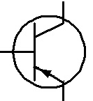
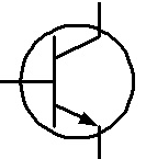
Schematic symbolsThe symbol for a BJT transistor is a little more complicated than for other components, that's because there are three legs for a start, and they come in two varieties, NPN and PNP.
We'll start with the emitter leg, if you think back to the diode, the symbol for that was an arrow with a bar, the arrow pointed to the N type silicon,
The part of the symbol that shows the emitter is an arrow, the arrow points to the N type silicon.
so on an NPN transistor the arrow points outwards from the base (because the base is P and the emitter is N), on a PNP type the arrow points inwards (because the emitter is P and the base is N)
The Base is a thick straight line.
the collector is an angled straight line.
so here is the symbol for a NPN transistor (remember the arrow point out)
And here is the symbol for the PNP type transistor (remember the arrow points in)