http://ah-screwit.blogspot.com/2012/10/electronics-lessons-making-gates.html
This post was a bit simplistic, but the logic was easy to follow, the idea that a transistor would conduct when on. (effectively being able to sink current from the output connecting the input of whatever came next to ground.) -or the transistor could be off, meaning not conducting so the output was connected to Vcc and the output was high.
This was the basic block of all the gates saying that we could run transistors in series to make the NOT gate into a NAND gate, or provide two connections to the base to make a NOR gate.
The trouble is, whilst in theory this will work, in practice there is not enough voltage gain, and over a series of make stages the signal will become weak.
The long and the short of it is that these simple single transistor gates are not real gates at all.
When I was talking about binary reduction and saving gates, you may think so what, I saved a NOT gate, that's only 1 transistor. but in reality. it's actually 4 transistors:
What you see here in a NOT gate.
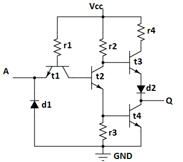
But it works a bit like this.
With a logic Low at the input.
T1 is clearly on, it's base is connected to Vcc,
Current flows from the base of T1 to the emitter, and flows to the logic low (ground).
the base of T2 is low, so T2 is off,
Since T2 is off we can see that the voltage at the emitter of T2 is low, so T4 is off, (output is not connected to ground through T4)
we can also see that since T2 is not conducting that the voltage at T2 collector is high, this is the base of T3, so T3 is on, conducting in the saturation region, and thus the output is high.
Logic low at input = Logic high at output.
Now consider what happens when the input is high.
T1 base is still connected to Vcc, so this transistor is still on and conducting, but this time rather than voltage flowing to ground at the input voltage must flow to ground through the base of T2, out the collector of T2, and to ground through R3.
so the Base of T2 is high, this turns T2 on.
this makes the T2 collector low and thus T3 it not on.
it makes the base of T4 high, so T4 is on. and connecting the output to ground.
logic high at input = logic low at output
So you see saving 80 not Gates doesn't save 80 transistors, it saves 320 transistors.
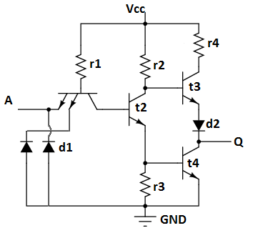
NAND
Funnily enough, with the basic transistor NAND gate we just stuck a transistor in series with the transistor making the NOT gate, now we put a second emitter in parallel with the first emitter.
We can't just put a transistor in series of parallel so we use a second emitter, (which is essentially just a second doped region on the silicon substrate.
This works exactly the same as the not gates, but instead of the base current for T2 being either grounded or supplied by THE (singular) input, it's not possible for it to be grounded by either input.
No comments:
Post a Comment