First we'll start with the NOT gate.
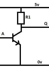
When the base of the transistor is bought high into the saturation region, the transistor conducts, and the collector is connected to ground.
When the base of the transistor is low, (in the cut-off region) the collector of the transistor is connected only to the Vcc voltage through the resistor, and thus the output of the circuit is high.
NAND
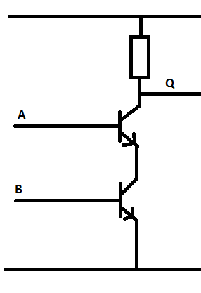
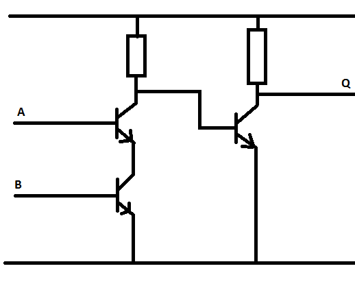
It might seem like it's going a little out of order to do the NAND gate next, but it's a very simple addittion to the NOT circuit.
The NOT circuit pulls the output low by providing a path to ground when the transistor is on, the NAND gate works just like this, except there are two transistors that have to be on to provide that path to ground, and those transistors are in series.
AND
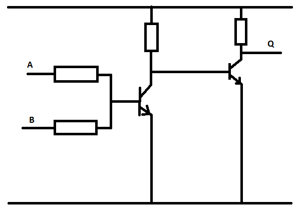
The output of the NAND gate is the inverse of the AND gate, and visa versa, to make an AND gate (when the output is high when both inputs are high) all we do it put a NOT gate following a NAND gate!
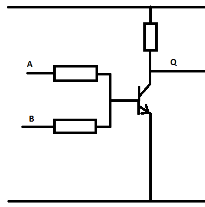
I said earlier that you could create a NOR gate just like a NAND gate, but instead of having the transistors in series have them in parallel.
You can also just have the base of transistor 1 able to be brought high by either input.
in this scenario the inputs are isolated from each other with the use of resistors.
Just as we turned a NAND gate into an AND gate with an inverter circuit (NOT gate) we do the same to turn the NOR gate into an OR gate.
http://ah-screwit.blogspot.co.uk/2012/09/electronics-lessons-making-gates-from.html
No comments:
Post a Comment